


PCB Layout and Analysis
PCB Layout and Analysis or Custom PCB Design Services is a product design process involving high-level engineering tools for board design. PCB Layout and Analysis is the point in a design stage at which all the design decisions made earlier come together and where unforeseen problems related to PCB Design Analysis Services like performance, power distribution analysis, signal integrity, thermal analysis and noise mismatching make themselves known and have to be resolved. Mistral is among the leading custom PCB Design companies in Bangalore. The team has over 25 years of experience in offering PCB Design Analysis Services. From PCB schematic design and PCB board layout to testing, validation, and certification, Mistral provides full range of PCB design services.
PCB Layout and Analysis
Mistral’s expertise in PCB Layout Design services cover complex multi-processor, MIL-STD-compliant, multi-layer boards, Highly dense and complex small footprint PCBs with proven design methodologies, processes and quality checks. Mistral has an experienced Custom PCB Design Services team that deliver world-class PCBA that are certifiable, deliver highest performance, manufacturable, low cost and thermally-efficient. We have been providing custom PCB design services and PCB Layout and Analysis services to Govt, Public and Private sectors in India and abroad for the past two decades. Mistral is among the leading Board and PCB Design companies in Bangalore offering custom PCB Design Services or PCB Design Analysis Services services consists of award-winning high-speed, digital and mixed-signal PCB layouts for VME, VPX, cPCI, PCIe, XMC bus and custom architectures, which have been deployed for various consumer, industrial, aerospace and defense applications.
PCB Layout Design Services
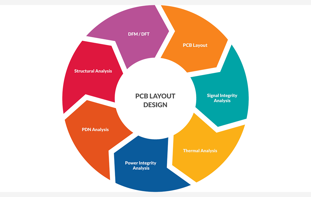
As part of our Custom PCB Design services, we also offer PCB reverse engineering in case of lack of documentation and re-engineering services to fix flaws and/or to optimize existing PCB designs for cost of obsolescence management. Mistral’s custom PCB design services help customers get to market faster with experienced PCB engineers ensuring performance and manufacturability. Our PCB layout design services team has designed & deployed over 10,000 PCBs in the market, including 100+ MIL standard Class-3 PCB and HDI PCB assemblies. Our PCB Design Analysis Services includes Library management, PCB Layout and Analysis, Power Integrity Analysis Services, Signal Integrity Analysis Services, Structural Analysis Services and Thermal analysis Services. Click here to read on blog on Fundamentals of Printed Circuit Board Design and Brief on HDI PCB Technology.

Expertise

Library Management
- Library Management for custom PCB Design Services covering
- IEEE based schematics symbol creation or custom
- IPC7351 PCB Land pattern method
- Footprints for least, maximum or nominal
- Component management

Custom PCB Design Services
- RF and Antenna PCBs
- High Density Interconnects (HDIs) PCBs
- Multi-layer PCBs (up to 32)
- Flex and RigidFlex

Signal Integrity Analysis Services
- Up to 10GHz simulation
- Pre SI simulation
- Topology & stackup
- Post SI simulation
- Report generation
- Power Distribution Network Analysis or Power Integrity Analysis Services

Thermal Analysis Services
- Air and conduction cooled
- Power Distribution
- 2D/3D Analysis
- Placement Management
- Report Generation

DFM/DFT
- Class2 and Class3 Specifications
- PCB Design Services with Yield improvements
- Support for automated/semi-automated testability
- Test coverage improvements
- Cost Reduction

Manufacturing Support
- Manufacturing support for custom PCB Design Services
- ODB++, RS274X
- Component, paste and assembly drawings
- 3D data for mechanical validation
Library Management
- Library Management for custom PCB Design Services covering
- IEEE based schematics symbol creation or custom
- IPC7351 PCB Land pattern method
- Footprints for least, maximum or nominal
- Component management
Custom PCB Design Services
- RF and Antenna PCBs
- High Density Interconnects (HDIs) PCBs
- Multi-layer PCBs (up to 32)
- Flex and RigidFlex
Signal Integrity Analysis Services
- Up to 10GHz simulation
- Pre SI simulation
- Topology & stackup
- Post SI simulation
- Report generation
- Power Distribution Network Analysis or Power Integrity Analysis Services
Thermal Analysis Services
- Air and conduction cooled
- Power Distribution
- 2D/3D Analysis
- Placement Management
- Report Generation
DFM/DFT
- Class2 and Class3 Specifications
- PCB Design Services with Yield improvements
- Support for automated/semi-automated testability
- Test coverage improvements
- Cost Reduction
Manufacturing Support
- Manufacturing support for custom PCB Design Services
- ODB++, RS274X
- Component, paste and assembly drawings
- 3D data for mechanical validation
Block Diagram
HDI, Flex and Rigid based Custom PCB Design Services that include
SUBSCRIBE TO OUR NEWSLETTER

Signup for our Newsletter to get the latest news on Products and Services