

Brief on High Density Interconnect (HDI) PCB Technology
Over the past couple of decades, we have seen electronic products and other consumer electronic devices reducing in weight and size while improvising phenomenally in speed, performance, and power consumption, and with no loss of quality or functionality. High-Density Interconnect (HDI) PCB Technology is one of the highlights of this transformation.
What is HDI PCB?
In the PCB design world, HDI PCB refers to the High-Density Interconnect PCB. The HDI PCB is a printed circuit board with a comparatively higher wiring density per unit area when compared with a conventional board. These compact, lighter in weight and size, and cost-effective HDI PCBs include high-density attributes like microvias, blind and buried vias, fine lines and spaces, sequential lamination, and via-in-pad techniques that help reduce size and weight, as well as enhance the electrical performance of embedded devices.
The HDI PCBs utilize thin materials and minimum layers for their composition compared to standard PCB boards, increasing the performance and efficiency of the HDI PCB boards. Hence, these circuit boards are ideal for complex small form-factor designs.
Different kinds of Vias in PCB
Vias are a tiny conductive hole that connects multiple layers in a PCB and allows signals to flow through them easily. Depending on the functionality of a PCB, four different types of vias are drilled into a PCB, namely: Through Hole vias, Blind Vias, Buried Vias and Microvias.
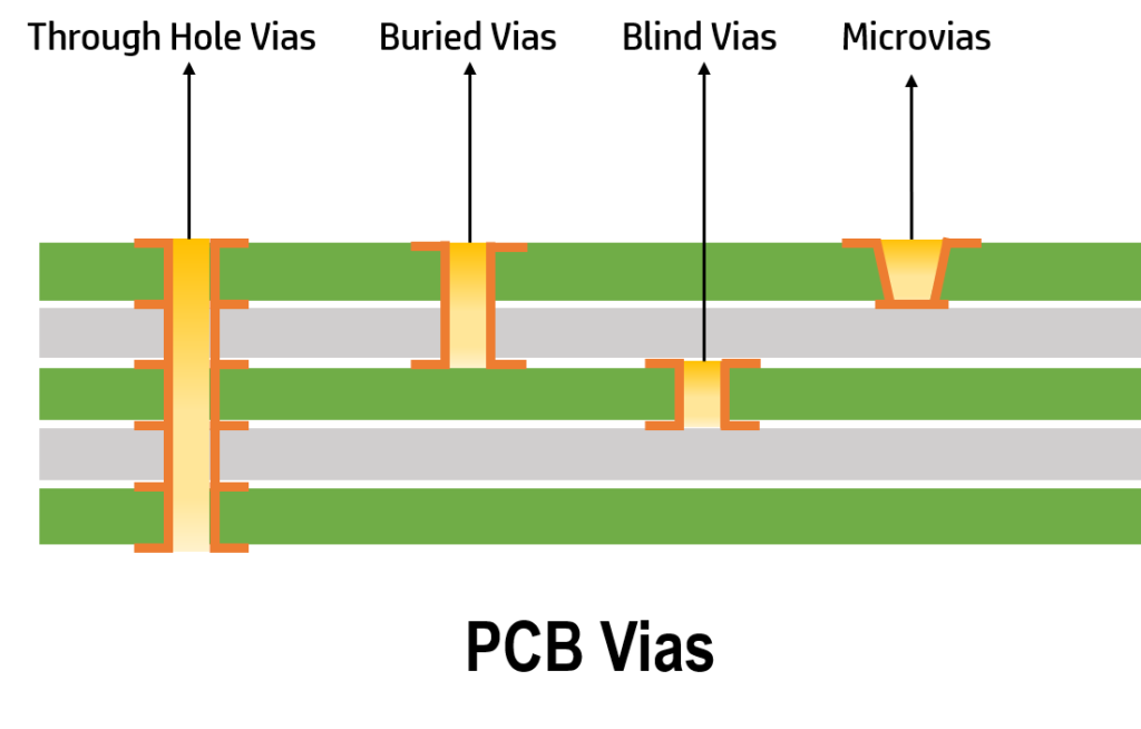
- Through-Hole Vias – It is a hole pierced using a drill or laser through the PCB from top to bottom connecting all the layers of the multi-layer PCB. The Through-hole PCB is easy to construct and are the most cost-effective type of vias. The Through holes are further divided into Plated Through (with copper pads) Holes and Non-Plated Through Holes (without copper pads).
- Blind Vias – A type of via where a hole is pierced using a drill or laser to connect the external layer of multi-layer PCB to the internal layer. Since the hole is visible only on one side of the PCB board, it is called Blind via. This type of via is difficult to construct and are expensive.
- Buried Vias – A via that connects two internal layers of multi-layer PCB. This via is always inside the printed circuit board and are not visible from the outside. Therefore, it is called buried via. The buried via is also an electroplated hole that needs a separate drill file. The layer count in a buried via is even in number i.e., 2, 4, 6, and on.
- Microvias – It is the smallest vias or holes with a diameter less than 150 microns, drilled using a laser. Microvias are most commonly implemented in HDI PCBs, usually to connect one layer of the PCB to its adjacent layer and have a very small diameter in comparison to the mechanically drilled vias such as through-hole. Due to their size and ability to connect one layer to an adjacent layer, they enable denser printed circuit boards with more complex designs.
Lamination process and the different types of HDI PCB stack-ups
HDI PCBs are multilayer boards that are constructed with densely routed layers and the boards are held together through a lamination process. These layers are electrically interconnected using different types of vias. The process of lamination begins with the etching of the inner copper layers. Later they are separated by partially cured laminates and stacked like a book with layers of prepreg on the top and bottom. The stack-up is then pressed and heated enough to liquify the prepreg. These liquified prepregs cool down and stick the layers together.
For blind and buried vias stack-ups the PCB will undergo several numbers of sequential laminations. The more the number of laminations, the costlier will be the board. To increase routing density, designers increase the number of layers, producing a complex stack-up. Manufacturers use sequential lamination processes to fabricate such complex designs.
Some of the common types of stack-ups are:
- HDI PCB (1+N+1): This is the simplest HDI design structure suitable for BGA with lower I/O counts. It has a fine line, microvias and registration technologies capable of 0.4 mm ball pitch, excellent mounting stability and reliability, and may contain copper filled via. It is a qualified material and surface treatment for a Lead-free process. Some of the examples include a Cell phone, UMPC, MP3 Player, PMP, GPS, Memory Card, etc.
- HDI PCB (2+N+2): This is a moderate complex HDI design structure that contains 2 or more build-up of high-density interconnection layers which allow the conductors on any layer of the PCB to be interconnected freely with copper filled stacked microvias structures. These structures are commonly seen in challenging designs that demand high-level signal transmission performance. They are suitable for BGA with smaller ball pitches and higher I/O counts and can be used to increase routing density in a complicated design while maintaining a thin finished board thickness. Some of the examples include smartphones, PDA, game consoles, and portable video recording devices.
- Any Layer HDI PCB: This is the most complex HDI design structure where all the layers are high-density interconnection layers which allow the conductors on any layer of the PCB to be interconnected freely with copper filled stacked microvias structures. This structure provides a reliable interconnect solution for highly complex large pin-count devices, such as CPU and GPU chips utilized on handheld and mobile devices while producing superior electrical characteristics. Some of the examples include smartphones, ultra-mobile PC, MP3, GPS, Memory cards, and small electronic devices.
Advantages of HDI PCBs
- HDI PCBs provides designers with the freedom to design and place more components on both sides of the PCB. This is due to the higher wiring density with finer track arrangements on PCBs.
- With the use of microvias and via-in-pad technology, the components are densely packed with versatile routing which results in faster transmission of the signal and better signal quality.
- The HDI PCB boards allow you to pack all functions in one board rather than using several boards as in standard PCBs. This results in reducing the size and overall costs compared to the traditional PCBs.
- The HDI PCB boards are highly reliable due to the implementation of stacked vias which make these boards a super shield against extreme environmental conditions. Hence the boards are highly reliable.
- Laser drilling produces smaller holes and improves the thermal properties of the board.
Applications
- Healthcare industry – HDI PCBs have shown tremendous possibilities in the healthcare and medical fields. For example, tiny, implanted devices such as pacemakers, portable X-Rays and external devices such as hearing aids use the HDI technology.
- Consumer devices – Due to the compact nature, the HDI PCBs are used in most consumer products such as smartphones, tablets, laptop computers, touch screen products and home appliances.
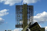
- Aerospace – The HDI PCBs can withstand extreme environmental conditions making it feasible to be utilized in electronics design for missile systems, aircraft, and defense applications.
- Wearables – Due to the size of HDI PCBs, they are widely used in wearable technologies. F0r example, VR headsets, smartwatches, smart clothing, and more.
Future of HDI Technology
HDI Technology is taking PCB design to the next level! It is being widely adopted in the consumer electronics sector and has high growth potential in the automotive industry. With the advancements in printed circuit boards, the HDI technology market looks promising with opportunities in various industries such as IT & Telecommunications, industrial electronics, and consumer electronics.
According to the Report Linker, the HDI Printed Circuit Boards market is expected to reach an estimated $16.4 billion by 2025 with a CAGR of 6% to 8% from 2020 to 2025. The major drivers for the global HDI PCB market are a miniaturization of size and lower weight of electronic devices, increasing demand for high efficiency, and high-performance devices and growing sales of the consumer electronics market.
The analyst forecasts that within the HDI PCB market; a smartphone will remain the largest end-user industry due to the increasing demand for high-performance PCB and growing demand for more space in smartphones for larger batteries. The HDI technology has influenced the automotive industries with smaller, lighter electronics creating substantial space and reducing vehicle weight eventually providing a greater driving experience. Also, due to advancements in automotive electronics, sophisticated safety systems, autonomous driving, and the miniaturization of electronic devices, the automotive industry is expected to witness the highest growth over the forecast period. The advent of autonomous vehicles connected cars and 5G technology is also going to have a huge impact on the global HDI PCB market.
Conclusion
The advancement of High-Density Interconnect PCB Technology in PCB layout and analysis is being driven by the miniaturization of components and semiconductor packages which support a variety of advanced features that are getting utilized in revolutionary new products in applications such as wearable electronics, touch screen computing, compact, small footprint gadgets, defense and aerospace. If you are looking for a technology that allows you to work anywhere, anytime, boosting your efficiency, then this is it!
With 20+ years of experience in PCB Custom Design and development, Mistral provides cost-effective HDI PCB designs that include microvias, blind and buried vias, fine lines and spaces, sequential lamination, via-in-pad techniques that help reduce size and weight, as well as enhance the electrical performance of embedded devices. Our HDI PCB Layout Services includes Library management, PCB Layout and Analysis, Power Integrity Analysis Services, Signal Integrity Analysis Services, Structural Analysis Services and Thermal Analysis Services.