

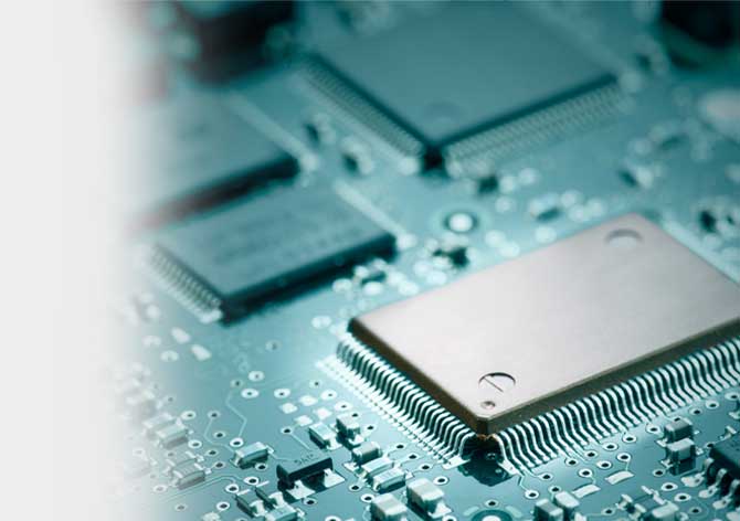
High Density Interconnect PCB (HDI PCB)
Cost-effective High Density Interconnect PCB (HDI PCB) designs that help reduce size and weight, as well as enhance electrical performance of embedded devices.
OVERVIEW
Over the past couple of decades we have seen consumer and other electronics devices reducing in weight and size while improving phenomenally in speed, performance and power consumption. HDI PCB Technology is one of the leading reasons for this transformation. High Density Interconnect PCB Technology enables more space on a printed circuit board, while making them more efficient and allowing faster transmission.
What is HDI PCB?
HDI PCB Layout has a higher wiring density per unit area than conventional PCBs and are ideal for complex small form factor designs. A High Density Interconnect PCB contains blind and/or buried vias and quite often contains microvias of .006 or less in diameter. This advancement in PCB layout and analysis is being driven by the miniaturization of components and semiconductor packages which support a variety of advanced features that are getting utilized in revolutionary new products in applications such as wearable electronics, touch screen computing, compact, small footprint gadgets, defense and aerospace.
Mistral’s team has extensive experience in designing cost-effective High Density Interconnect PCB (HDI PCB) designs that help reduce size and weight, as well as enhance electrical performance of embedded devices. We design cost-effective High Density Interconnect PCB using microvias, blind and buried vias, fine lines and spaces, sequential lamination, via-in-pad technology based techniques. HDI PCB design and manufacturing requires an advanced level of technical expertise. Our eco-system of PCB manufacturing companies and collaboration with Avalon Technologies, a global ESM company, enables us to provide our customers with a seamless product and system design experience. Our expertise in High Density Interconnect PCB includes handling the power integrity impact while designing using HDI PCB technology. This includes the effects of the mounted inductance of decoupling capacitors, changes in plane performance due to reduction in perforation from chip pin-outs, and the inherent plane-capacitance changes from using dielectrics of various thicknesses.
EXPERTISE
- Selection of HDI PCB layout techniques based on Size, Performance and Components
- Innovative design methods in Fine Pitch Micro BGA designs
- Up to 0.37mm BGA pitch designs with 2 mil/2mil track/spacings
- HDI PCB Technology Designs with stacked and staggered micro-vias
- Board/System level Signal Integrity, EMI/EMC & Thermal analysis
- Signal performance analysis for Reflections, Timing, BER, EYE opening
- DC drop analysis in power supply rails
- Handling power integrity impact while designing using High Density Interconnect PCB techniques
RESOURCES
-
Blog
Brief on High Density Interconnect (HDI) PCB Technology
-
Blog
Fundamentals of Printed Circuit Board
-
Case Study
Design and Development of High-Definition, Rugged Digital Video Recorder using HDI PCB Technology


-
Case Study
HDI PCB layout based Small-footprint Hands-free Headset with 15 inch Virtual Display
-
Product Brief
820 Nano SOM based on Qualcomm SnapDragon SD820 SoC

-
Product Brief
i.MX6 Nano SOM based on Dual/Quad i.MX6 SoC from NXP
-
Related Topics
Product Design Services
-
Related Topics
Small Form Factor Designs
-
Related Topics
Power Integrity Analysis
-
Related Topics
Signal Integrity Analysis
-
Related Topics
PCB Design Services